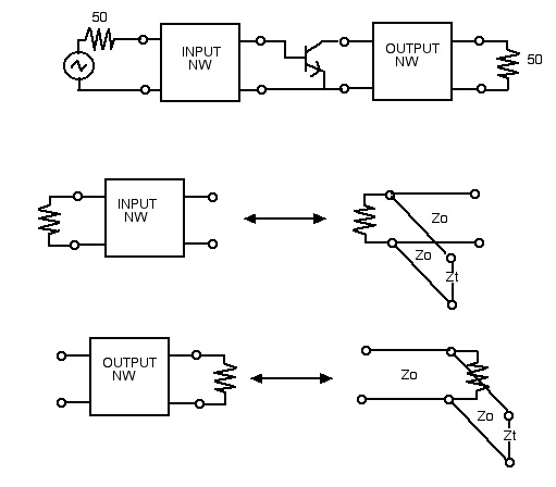
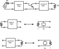
MATCH NETWORKS
The input and output match networks are simple two element L networks. They are chosen in the program to be implemented either as TEM microstrip line lengths or as L and C lumped elements. The input match NW transforms the 50 ohm source resistance into the design value of source impedance required at the device source port. The output match NW transforms the 50 ohm load resistance into the design load impedance required at the device load port.
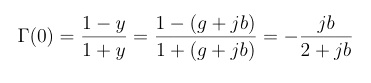
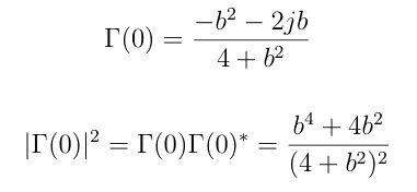
The implementations are depicted as transmission line elements but they can also be realized as lumped element Ls and Cs.
TEM TRANSMISSION LINE REALIZATION:
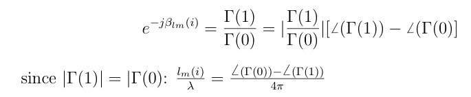
The stub terminations, ZT, can be opens or shorts but both are constrained to be of the same type. All main lines and stub lines are 50 ohm characteristic impedance. The 50 ohm terminating impedances are to be transformed via the matching networks to ZS and ZL respectively. The source and load reflection coefficients at the transistor planes, denoted by GammaS and GammaL respectively, have been previously determined by the program. It is required to find the lengths of the input and output cascade transmission lines and shunt stubs. Essentially the problem is a transmission line circuit problem worked in reverse, i.e., the input impedance is known and the imaginary part of the load impedance is to be derived (the real part is 50 ohm). Let Gamma(1) represent the reflection coefficient at the matching networks/transistor plane for either the input or output matching network. Let Gamma(0) stand for the reflection coefficient at the stub location. In this context, the arguments (1) and (0) stand for load position and generator position respectively in accordance with normal slotted line or Smith Chart usage. Converting to admittance and normalizing:
where g=1 is the normalized 50 ohm load conductance and b is the normalized stub input susceptance.
where
modulus is denoted by [ ]. Since only the phase of the reflection coefficient varies on an ideal lossless transmission line, we get:

After algebraic manipulation we get
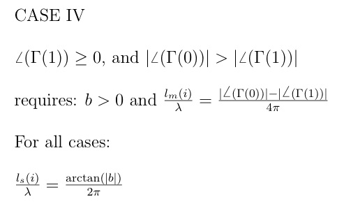
And C is always less than or equal to 1. The stub length is determined from the calculated susceptance. A matching network realization may be obtained with either short or open circuit termination; either type has its advantages. The open stub has a better defined end effect and development trimming is easy to do. The short stub may result in a simpler bias circuit. The determining factor may be the computed frequency response (easy to see with QUAMP) since the circuit effective loaded Q factor will be different for the two types.
For the open stub, the electrical length is given as:
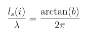
where I = 1,2 for source or load.
The main line length from the stub position to the device measurement plane is determined from the ratio of respective reflection coefficients:
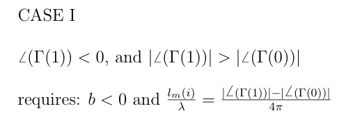
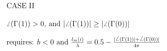
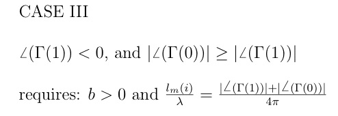
Since the direct calculation of the line lengths entails ambiguities in terms of trigonometric quadrant and required progression from generator to load position, it is necessary to include appropriate algorithms. There are four possibles cases as depicted on the Smith Chart:
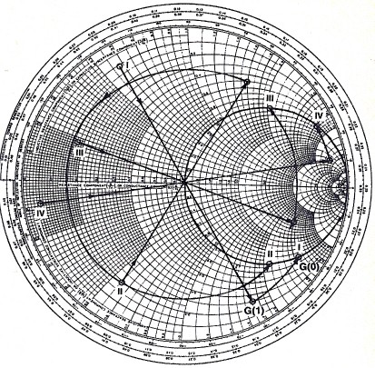
It is noted that the starting point reflection coefficients on the Smith Chart represent impedance quantities. The above definitions, however, are for the admittance values and correspond to the points at the arrowhead prior to rotation to the unit circle.
LUMPED ELEMENTS REALIZATION:
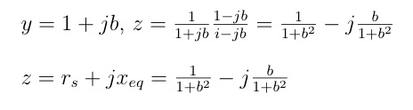
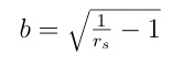
This situation is most readily analyzed by considering a unit source (load) conductance in parallel with a to be found susceptance. The condition for the determination of the susceptance is that this network be transformed to the requisite source (load) impedances.
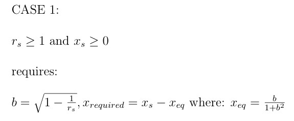
There are four possible cases equivalent to that for the distributed elements realization:
Marcus Staloff
© 2013