DESIGN EXAMPLES
Design examples
This section gives some working examples to provide insight into the appli- cation's ease of use and specific results which validate its performance.
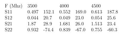
As a first example, a design at a center frequency of 4.3 GHz is shown. The s parameters for the device are given in the following table:
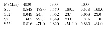
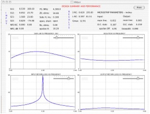
The microstrip parameters for a microstrip realization are dielectric constant of 10.2, substrate height of 0.100 inches, and open circuit stub terminations.
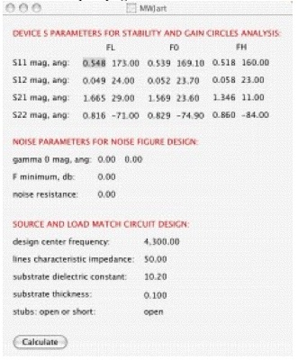
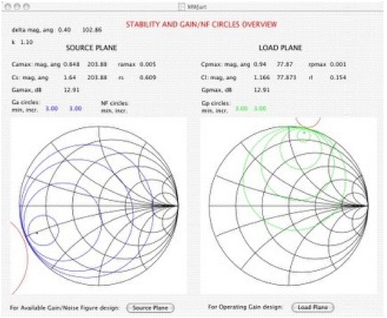
The overview page:
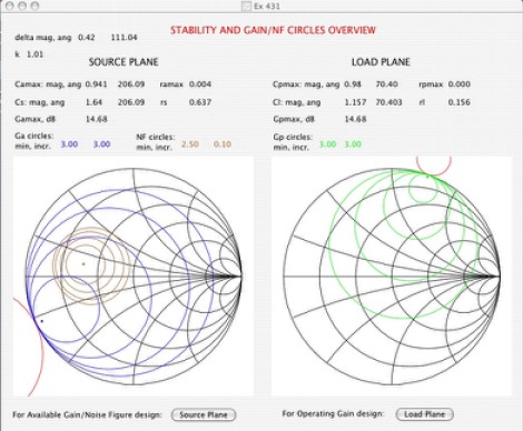
On this page one can get some insight with respect to design placement on the Smith Chart and stability considerations. Design for specific noise figure is not a factor in this design so that these considerations may guide the choice. A load plane design is chosen.
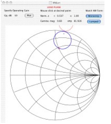
The load plane page:
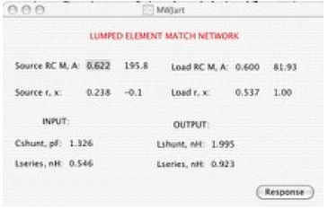
The selection bullet gives a normalized load impedance of 0.537+j1.0 ohms corresponding to a load reflection coefficient of 0.6 magnitude at an angle of 81.93 degrees. The output matching network will transform the real load of 50 ˝ to this required device load impedance. The input matching network design will transform the real source impedance of 50 ˝ into the conjugate of the device input impedance which results when the device is loaded with the specified load impedance.
The microstrip page: The results of the matching networks design for a microstrip realization is shown.

The lumped elements page:
The results page:
Lumped elements:
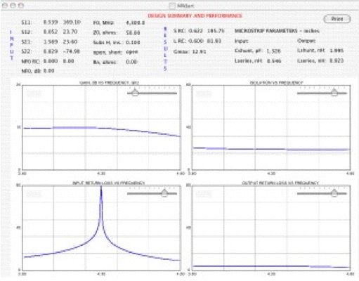
Typically, the lumped elements realization will exhibit broader band per formance because the transmission line elements have higher Q factor.
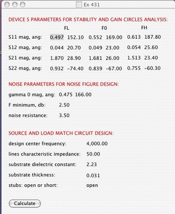
An example using a design from Microwave Amplifiers is shown in the fol lowing.
S parameters:
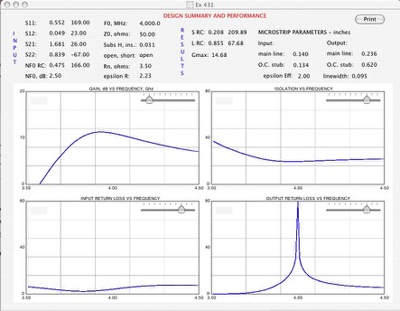
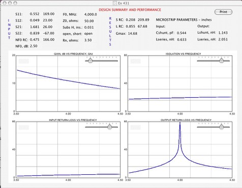
The microstrip parameters for a microstrip realization are dielectric constant of 2.23, substrate height of 0.031 inches, and open circuit stub terminations.
The data input page:
The overview page:
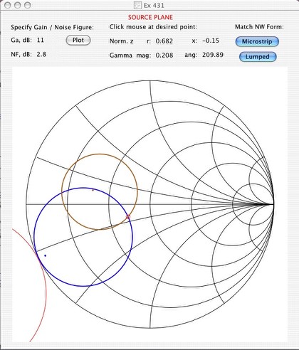
The selection bullet gives a normalized source impedance of 0.682-j0.15 ohms corresponding to a load reflection coefficient of 0.208 magnitude at an angle of 209.89 degrees. This chosen operating condition is for a gain of 11dB and a noise figure of 2.8 dB. The input matching network will transform the real source impedance of 50 ˝ to this required device source impedance. The output matching network design will transform the real load impedance of 50 ˝ into the conjugate of the device output impedance which results when the device has the specified source impedance.
The microstrip page:

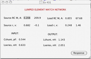
The lumped elements page;
The results page:
Microstrip:
Luimped elements:
References
M. Staloff, Computer-Aided Design and Analysis of Microwave Transistor Amplifiers, Microwave Journal, Vol. 30, No. 5, May, 1987.
S-Parameters, Circuit Analysis and Design, Hewlett Packard Application Note 95.
G. Gonzales, Microwave Transistor Amplifiers Analysis and Design, Prentice-Hall, Inc., Englewood Cliffs, NJ 1984.
T. T. Ha, Solid-State Microwave Amplifier Desgn, Wiley-Interscience, New York, 1981.
R. N. Ghose, Microwave Circuit Theory and Analysis, McGraw-Hill Book Co. Inc., New York, 1963.
Marcus Staloff
© 2013